PVD: Magnetronsputtern

About PVD

PVD.
PVD.

The term PVD (Physical Vapour Deposition-physical vapour deposition) stands for a large and still growing range of methods for thin film deposition, in which the atoms or molecules of the substance to be deposited are transferred from the source via vacuum to the substrate without chemical conversions. The oldest and in principle the simplest of these methods, thermal evaporation in a vacuum, is still widely used, but is gradually being pushed back by various plasma assisted technologies.

In the IGB, PVD is primarily used to complement (plasma) chemical surface technologies. As an application example, the improvement of adhesion of thin metal layers by plasma polymer deposition can be mentioned. At present, we have magnetron sputtering at our disposal; other PVD methods can be offered through cooperations, especially in the Fraunhofer POLO Group.

About Sputtering

Sputtering.
Sputtering.

About Sputtering

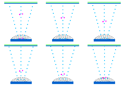
In sputtering, a glow discharge is generated in an argon atmosphere at low pressure, whereby the source of the material - the target - is the cathode. The Ar ions (magenta on the animation on the left) are accelerated by the electric field in the direction of the target and knock atoms out of the target, which deposit on the opposite substrate.

By applying a magnetic field in the target area, the efficiency of the process is dramatically improved.

Magnetron sputtering (also known as magnetron sputtering) can be used to sputter mainly non-magnetic metals and alloys. Sputtering is also possible of most other inorganic materials, albeit with increased effort.

The thickness of the coating is proportional to the discharge current and the deposition time and can range from a few nanometers to a few micrometers.

Among the advantages of this method, besides easy control and reproducibility of the deposition process, is the accurate transfer of the chemical composition from the source (the target) to the deposited layer.

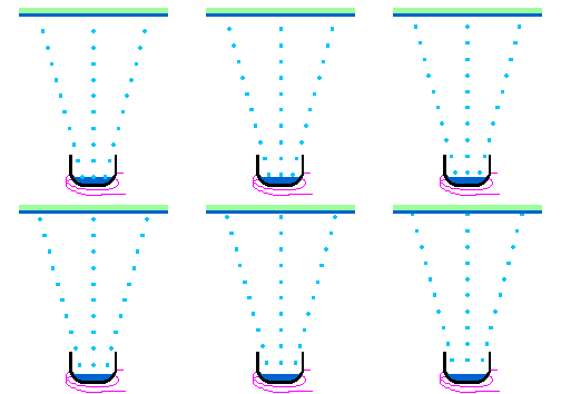
Magnetron sputtering system

Magnetron system.
Magnetron system.
  • Two magnetrons (for sequential deposition in multilayer systems)
  • Target diameter 90 mm
  • Currently DC sputtering; RF sputtering can also be implemented for electrically non-conductive substrates
  • Max. sample size approx. 100x100 mm
  • Additional station for plasma treatment

    The system is a self-construction and can be reconfigured or extended as required.